Epitaxy - Epitaxial Growth of Layer Structures
Epitaxy is a field of professional competence offered by Jenoptik. Devices based on Jenoptik epitaxial wafers in the Al-Ga-In-As-P material system have proven their quality in numerous products. Additional to our laser products, we provide customized epitaxy services in the production of thin semiconductor layer structures, i.e. epitaxy of layer structures on GaAs wafers. In accordance to your specifications, we are able to deliver epitaxial wafers with guaranteed high-quality epitaxial growth of layer structures on 2”, 3”, and 4” wafers.
Production of epitaxial wafers
We focus on layer structures for opto-electronic components which will be the basis for your state-of-the-art devices such as
- Laser diodes: wavelengths of 630 - 1,200 nm
- Surface emitters (VCSELs and VECSELs)
- Light-emitting diodes (RCLEDs and LEDs)
- Schottky diodes
- Detector structures
.jpg) |
| 2, 3 and 4 inch wafers |
|
|
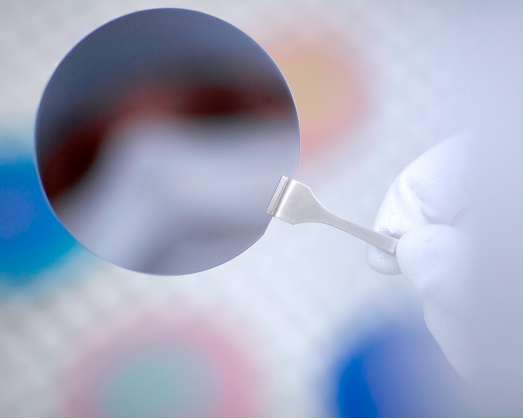 |
| Inspection of Wafer |
|
|
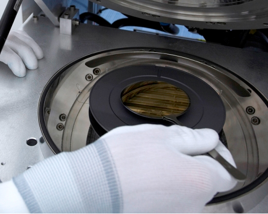 |
| Epitaxial Service |
|
|
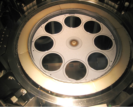 |
| Production Reactor for Epitaxial Service |
Our monitored MOCVD / MOVPE production process with tight quality control ensures consistently high quality from start to finish.
PDF Epitaxial wafer services (168 KB)
| Epitaxy product features |
Advantages |
- Epitaxial growth of layer structures in the Al-In-Ga-As-P material system
- High reliability
- Consistently high quality
- Wafers for various components
- Customized layer structures
|
- Short development cycles
- High flexibility
- Low development costs
- Short lead times
- Competitive prices
|
For any questions regarding our epitaxial services or for comprehensive consulting, please contact us. We are happy to assist you.
» To the terms & conditions
» To the company information


